Home / Factory

A factory you can ask questions about.

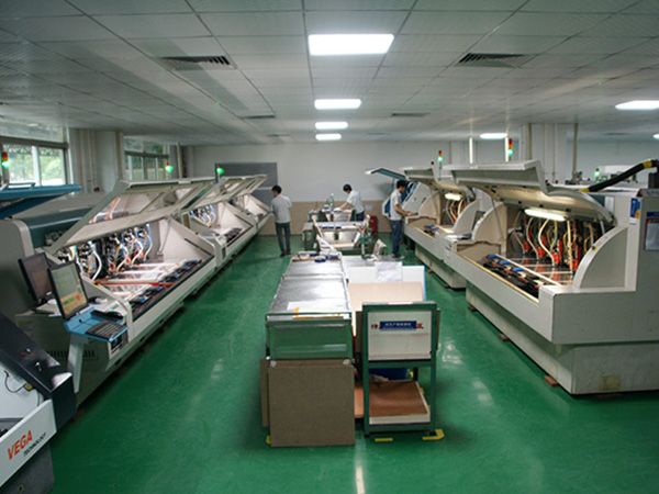
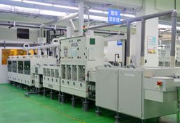
20,000 m² in Bao'an, Shenzhen. 300 people. 50,000 m² of board a month. The 45 machines listed and pictured below do the work.

20,000 m²Production floor at one site
300+Staff, including engineering and QA
50,000 m²Monthly output capacity
Class 100,000Cleanroom for imaging and lamination

Equipment

What's on the floor

Grouped by process stage, in the order a panel moves through the plant. Machine names match the ones on our production plan, so you can trace each step your board goes through.

StageEquipment
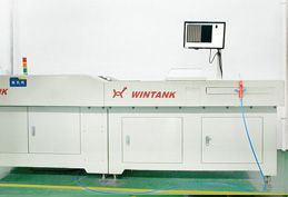
Imaging & patterningLDI direct imaging (inner and outer layer), CCD exposure for pattern and solder mask, automatic dry-film lamination, EIE photo-plotter, development lines
Drilling & routingCNC drilling, X-ray target drilling, depth-controlled drilling, back drilling, CNC routing, laser drilling for HDI microvias
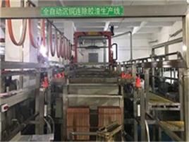
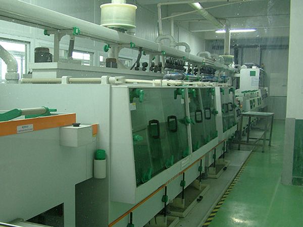
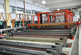
Plating & etchingAutomatic PTH lines, automatic pattern plating lines, vacuum etching, brown oxide line, vertical coating and baking
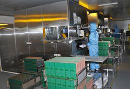
LaminationMultilayer press lines, inner-layer fusion, post-lamination bake, rigid-flex quick press, coverlay lamination
InspectionFilm AOI, AOI on inner and outer layers, automated visual inspection, hole verification, line-width measurement, 2D measurement
Electrical testOpen/short testers, four-wire low-resistance flying probe, dedicated fixture test for volume builds
LaboratoryMetallographic microscope, copper and coating thickness by X-ray, tensile tester, impedance tester, RoHS analyser, solderability testing

Workshop

44 machines, five process stages

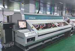
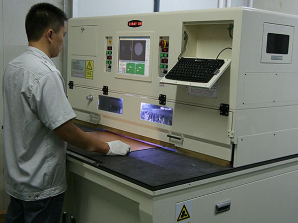
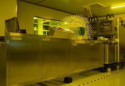
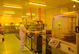
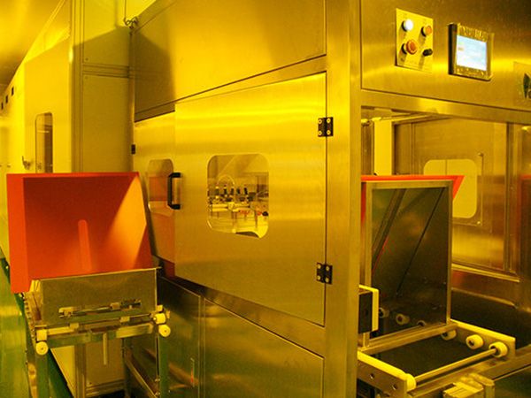
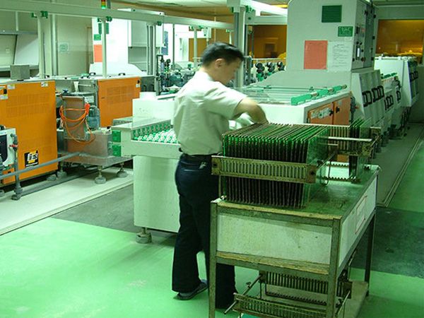
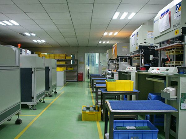
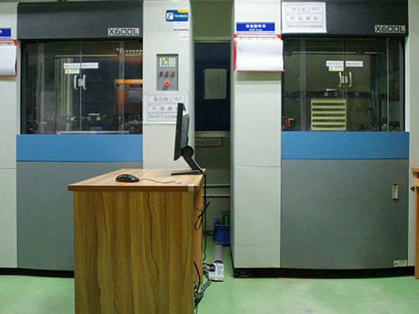
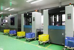
Every photo below was taken on our own floor, and the captions are the machines' actual names on our production plan. Cutting, imaging, plating, lamination, test and the lab — all under one roof.

Cutting, drilling & routing
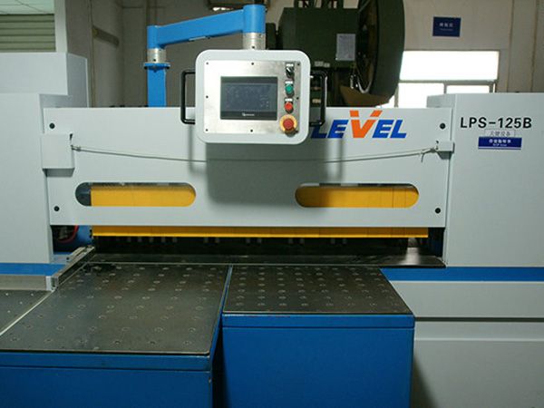
Automatic panel cutter at the Reach PCB plant
Automatic panel cutter
CNC drilling at the Reach PCB plant
CNC drilling
X-ray target drilling at the Reach PCB plant
X-ray target drilling
X-ray target punching at the Reach PCB plant
X-ray target punching
CNC routing at the Reach PCB plant
CNC routing
Hole verification, post-drill & final at the Reach PCB plant
Hole verification, post-drill & final

Imaging & patterning
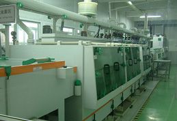
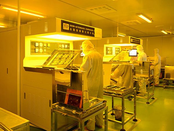
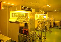
CCD automatic exposure at the Reach PCB plant
CCD automatic exposure
Circuit CCD exposure at the Reach PCB plant
Circuit CCD exposure
Solder-mask CCD exposure at the Reach PCB plant
Solder-mask CCD exposure
Circuit LDI exposure at the Reach PCB plant
Circuit LDI exposure
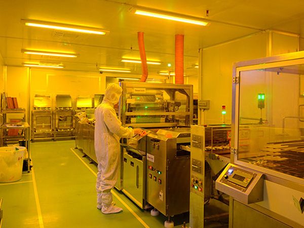
Inline LDI line at the Reach PCB plant
Inline LDI line
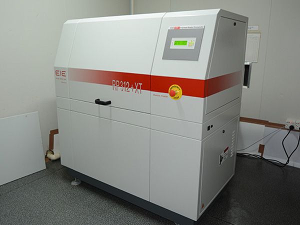
EIE photoplotter at the Reach PCB plant
EIE photoplotter
Automatic dry-film laminator at the Reach PCB plant
Automatic dry-film laminator
Automatic film pressing machine at the Reach PCB plant
Automatic film pressing machine
Dry-film lamination station at the Reach PCB plant
Dry-film lamination station
Vertical coater-baker line at the Reach PCB plant
Vertical coater-baker line
Developing machine at the Reach PCB plant
Developing machine
Solder-mask developing line at the Reach PCB plant
Solder-mask developing line
Pattern etching line at the Reach PCB plant
Pattern etching line

Plating & lamination
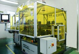
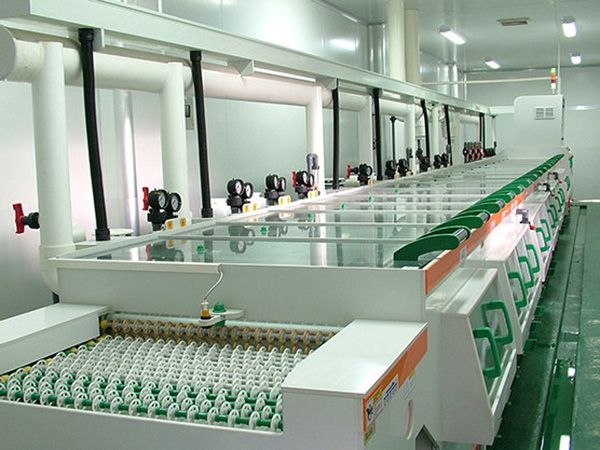
Automatic PTH line at the Reach PCB plant
Automatic PTH line
Automatic plating line at the Reach PCB plant
Automatic plating line
Automatic electroplating line at the Reach PCB plant
Automatic electroplating line
Brown oxide line at the Reach PCB plant
Brown oxide line
Inner-layer pre-lamination treatment at the Reach PCB plant
Inner-layer pre-lamination treatment
Inner-layer fusion machine at the Reach PCB plant
Inner-layer fusion machine
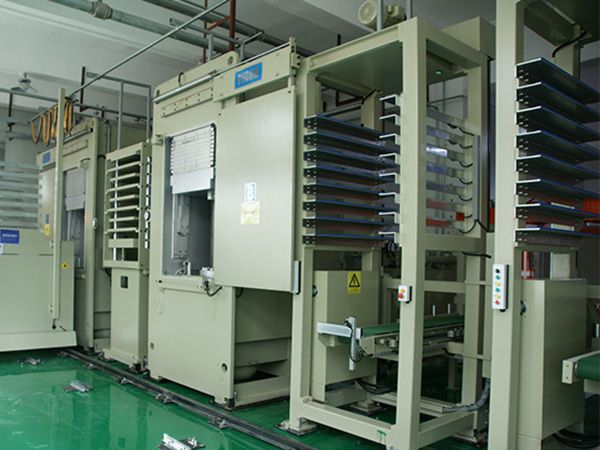
Multilayer laminating press at the Reach PCB plant
Multilayer laminating press
Lamination press at the Reach PCB plant
Lamination press
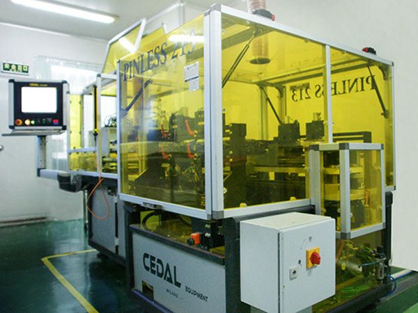
Automatic pinless alignment fusion press at the Reach PCB plant
Automatic pinless alignment fusion press

Inspection & electrical test
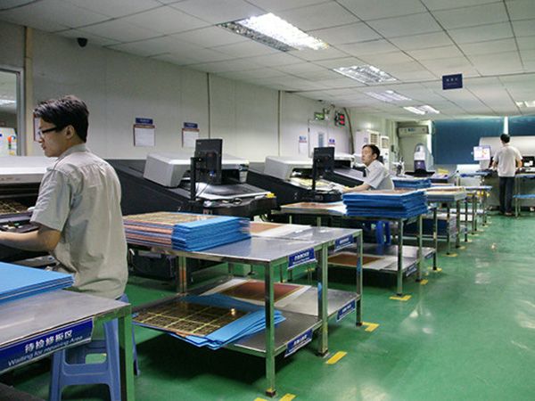
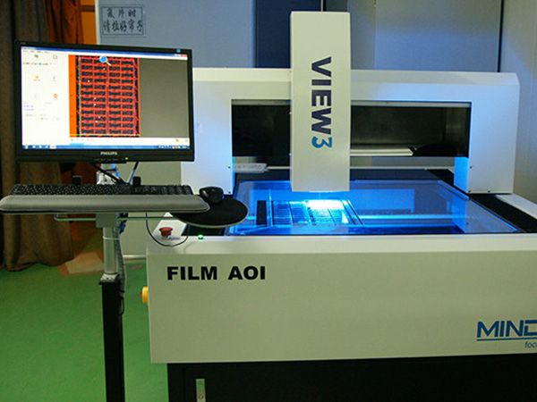
Film AOI scanner at the Reach PCB plant
Film AOI scanner
AOI machine at the Reach PCB plant
AOI machine
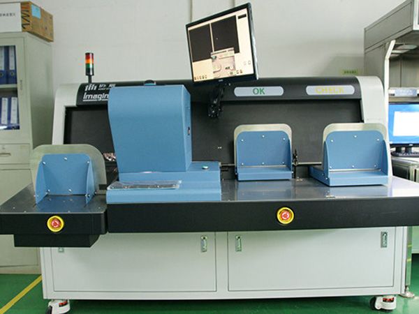
Automated visual inspection (AVI) at the Reach PCB plant
Automated visual inspection (AVI)
Film inspection scanner at the Reach PCB plant
Film inspection scanner
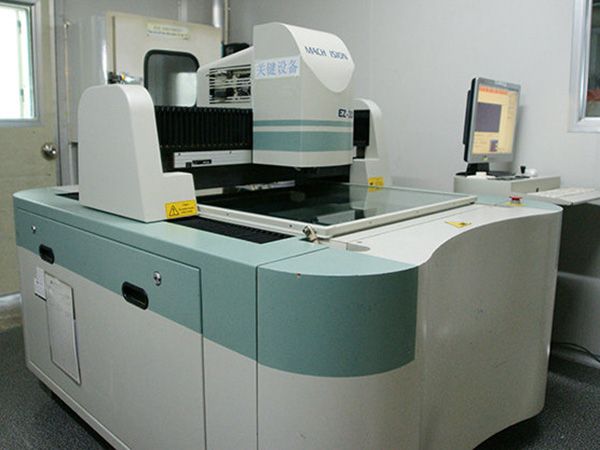
2D measuring machine at the Reach PCB plant
2D measuring machine
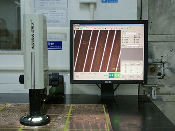
Line width & spacing gauge at the Reach PCB plant
Line width & spacing gauge
Open/short electrical tester at the Reach PCB plant
Open/short electrical tester
Four-wire low-resistance flying probe at the Reach PCB plant
Four-wire low-resistance flying probe
Flying probe tester at the Reach PCB plant
Flying probe tester

Laboratory

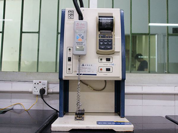
Tensile tester at the Reach PCB plant
Tensile tester
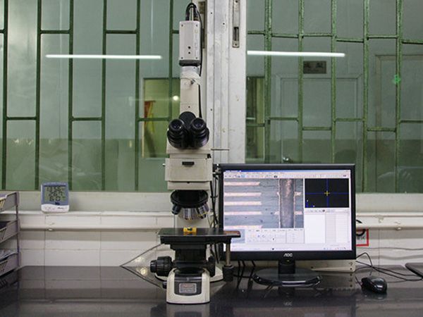
Metallographic microscope at the Reach PCB plant
Metallographic microscope
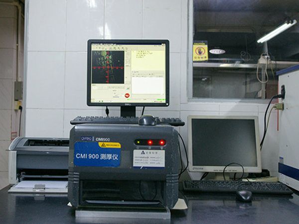
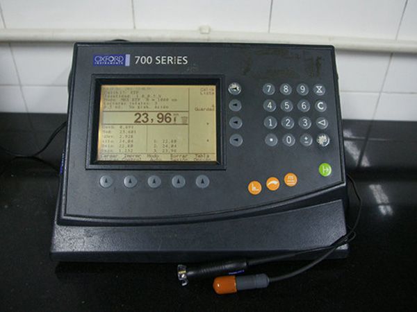
X-ray coating thickness gauge at the Reach PCB plant
X-ray coating thickness gauge
Hole copper thickness gauge at the Reach PCB plant
Hole copper thickness gauge
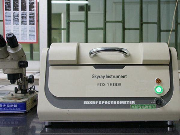
RoHS analyser (XRF) at the Reach PCB plant
RoHS analyser (XRF)
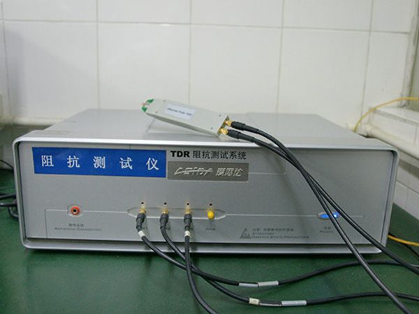
Impedance tester at the Reach PCB plant
Impedance tester
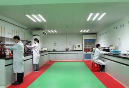
Physical laboratory at the Reach PCB plant
Physical laboratory

Traceability

Every board is traceable to its material lot

Material lots, process parameters, test results and inspection records are filed against each work order and kept on site.
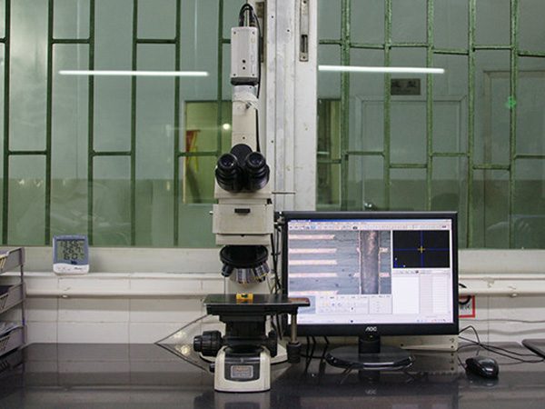
Metallographic microscope in the PCB laboratory
Metallographic microscope in the QA laboratory